LM-MG24 Module Specification
Overview
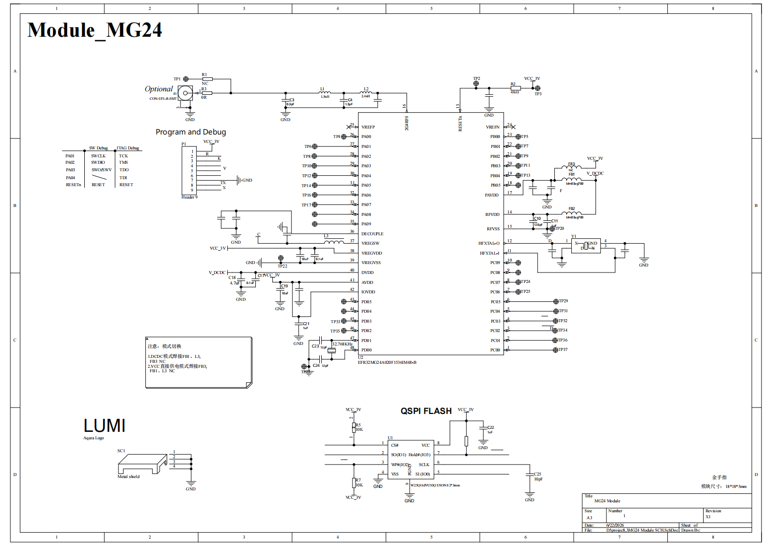
The Aqara MG24 module solution is an ideal mesh IoT wireless connectivity option, built on the EFR32MG24 chip featuring a Cortex®-M33 core with a maximum operating frequency of 78.0 MHz, up to 1536 KB of Flash memory, and 256 KB of RAM. It supports development of wireless communication technologies such as Matter, OpenThread, and Zigbee, and includes reserved IPx antenna interface and PCB antenna interface.
List of Hardware Resources
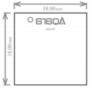
Module size: 18(±0.35) × 18(±0.35) × 5(±0.35) mm, SMD (36-pin) type
Wide operating voltage range: 2.0 V to 3.8 VDC
Optional antenna: IPX antenna or PCB antenna
System on chip:
- High-performance 32-bit 78.0 MHz ARM Cortex®-M33 is adopted, which processes signals using DSP instructions and floating-point operations
- 1536 kB flash, 256 kB RAM
Radio-frequency signal
- 2.4 GHz radio operation
- -105.4 dBm sensitivity @ 250kbps O-QPSK DSSS
- -105.7 dBm sensitivity @ 125kbps GFSK
- -97.6 dBm sensitivity @ 1 Mbps GFSK
- -94.8 dBm sensitivity @ 2 Mbps GFSK
Power dissipation
- 4.4 mA RX current (1 Mbps GFSK)
- 5.1 mA RX current (250 kbps O-QPSK DSSS)
- 5 mA TX current @ 0 dBm output power
- 19.1 mA TX current @ 10 dBm output power
- 156.8 mA TX current @ 19.5 dBm output power
- 33.4 μA/MHz in Active Mode (EM0) at 39.0 MHz
- 1.3 μA EM2 DeepSleep current (16 kB RAM retention and RTC running from LFRCO)
Introduction to the Hardware System
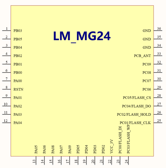
Module Pin Layout and Application
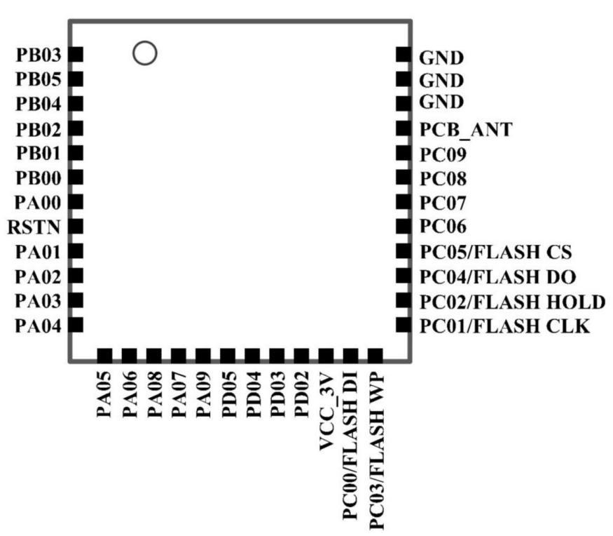
General-purpose I/O port
| Pin Name | Description | Special Instructions for Use as an Enabling Module |
|---|---|---|
| PB05 | GPIO | Reset user MCU, active low. |
| PB03 | GPIO | It is used as the wake-up port in low-power devices. The user's MCU wakes up the enabling module and connects an external 100K pull-up resistor; if the device is not a low-power device, it can be left unconnected. |
| PB01 | GPIO | As an ISP function, it connects to the I/O ports of the user's MCU and is used for OTA updates of the user's MCU. |
| PB00 | GPIO | Used as the wake-up port in low-power devices. The empowerment module activates the user's MCU. It needs to be connected to the external interrupt port of the user's MCU, and an external 100K pull-up resistor should be connected. If the device is not a low-power device, it can be left unconnected. |
| PA05 | Module UART TX | The communication interface connecting to the user's MCU. |
| PA06 | Module UART RX | |
| VCC_3V | Connect to Power | Module power supply 3.3V VCC. |
| PC00 | FLASH_DI | Used for modding and hacking - 4M FLASH. |
| PC03 | FLASH_WP | |
| PC01 | FLASH_CLK | |
| PC02 | FLASH_HOLD | |
| PC04 | FLASH_DO | |
| PC05 | FLASH_CS | |
| PCB_ANT | 2.4 GHz RF input/output | A π network needs to be connected between the PCB antenna and the antenna port.(CLC). |
| GND | Connect to Ground | Module grounding GND. |
| The other unused pins are left floating. | ||
Function Debugging of I/O ports
| Order Number | Pin Name | Functional Description |
|---|---|---|
| 1 | VCC | Positive terminal of the power supply |
| 2 | GND | Negative terminal of the power supply |
| 3 | RSTN | Reset pin, the RESETn pin is internally pulled up to DVDD |
| 4 | PA09 | GPIO |
| 5 | PA08 | GPIO |
| 6 | PA03 | GPIO |
| 7 | PA02 | GPIO |
| 8 | PA01 | GPIO |
| 9 | PD05 | GPIO |
| 10 | PD04 | GPIO |
Packaging Requirements
Package name: CONNECT - PH - 2X5 - 1.27mm
The numbering of the solder pads is uniformly arranged as follows:
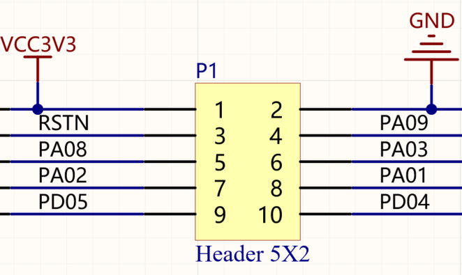
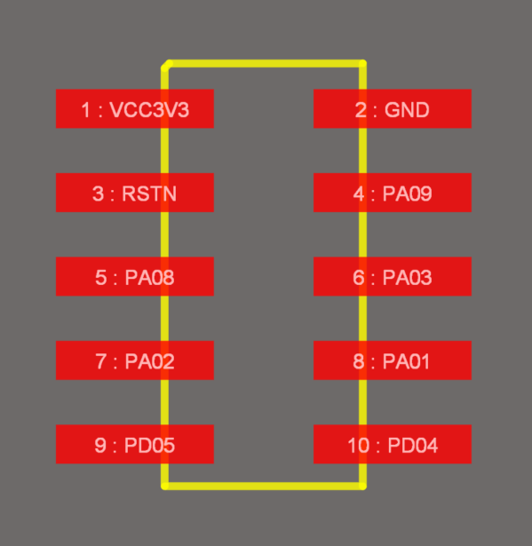
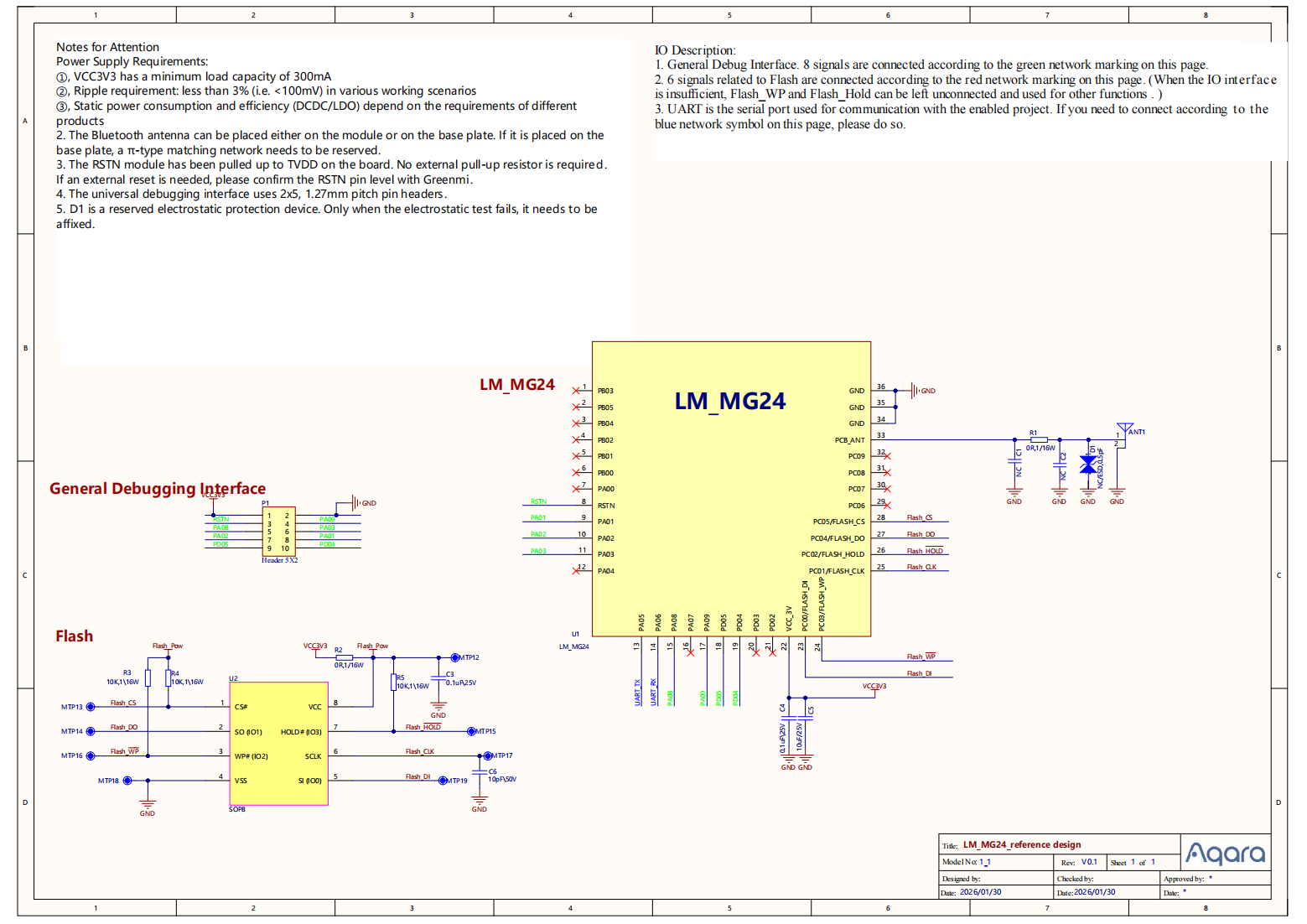
The RSTN reset is internally pulled up, so an external pull-up resistor is no longer required. Connecting a pull-up resistor externally may create a leakage current path, increasing the module's standby current.
Absolute Maximum Ratings
| Parameter | Symbol | min | max | Unit |
|---|---|---|---|---|
| Voltage on any supply pin | VDDMAX | -0.3 | 3.8 | V |
| Voltage ramp rate on any supply pin | VDDRAMPMAX | - | 1.0 | V/us |
| DC voltage on any GPIO pin | VDIGPIN | -0.3 | VDD+0.3 | V |
Reference Design Circuit
Module Size and Recommended Packaging
Schematic Diagram Packaging
PCB Package
Package name: BLE-MG24MODULE.
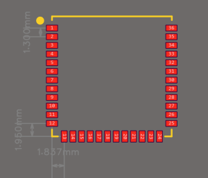
Single pad size: 1.6mm * 0.8mm, pad spacing 1.3mm
Attention
Flash Needs to be Reserved for Packaging on the Substrate
Aqara project generally has the requirement for external Flash expansion, and the corresponding required I/O ports are as shown in the table below.
| Pin Name | Pin Attribute | Flash Interface Function |
|---|---|---|
| PC00 | GPIO | FLASH_DI |
| PC03 | GPIO | FLASH_WP |
| PC01 | GPIO | FLASH_CLK |
| PC02 | GPIO | FLASH_HOLD |
| PC04 | GPIO | FLASH_DO |
| PC05 | GPIO | FLASH_CS |
The WP and HOLD signals of Flash can be pulled on the substrate. For the specific packaging and model of Flash that need to be reserved, please confirm with the hardware engineer of the Aqara.
Reference design:
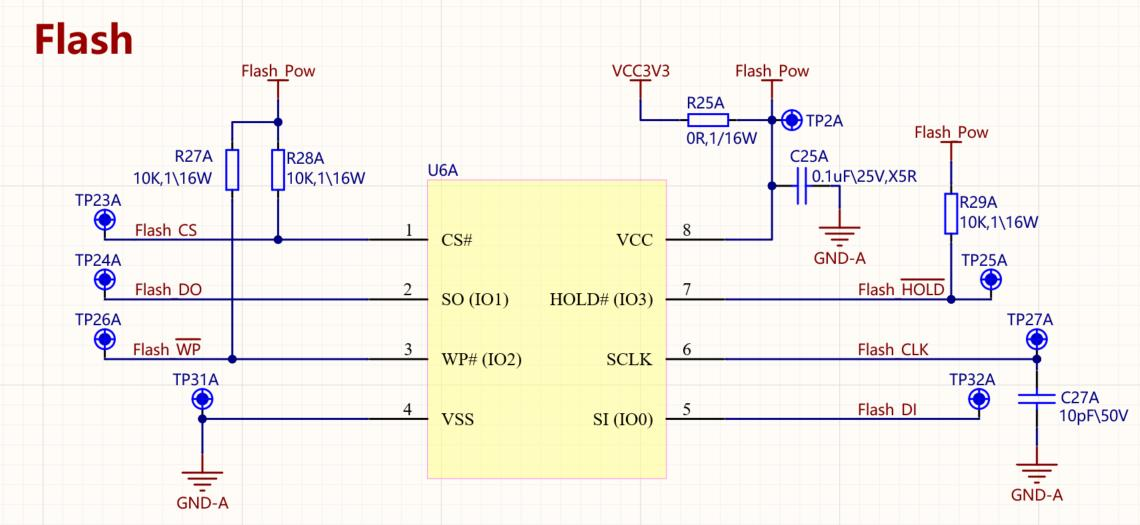
The table below lists the recommended flash models.
| Type | Vendor | Memory Capacity | Specification |
|---|---|---|---|
| ZB25VQ32ETJG | ZbitSemi | 4M byte | Nor Flash\32M-bit\2.3V-3.6V\SOP8-150mil\ |
| ZB25VQ32DDJG | ZbitSemi | 4M byte | Nor Flash\32M-bit\2.3V~3.6V\DFN8 2*3mm\ |
| ZB25VQ32DTJGR | ZbitSemi | 4M byte | Nor Flash\32M-bit\2.3V-3.6V\SOP8-150mil\ |
| PY25Q32HB-SSH-KR-SF | Puya | 4M byte | Nor Flash\32M-bit\2.3V |
| XT25F32FSOIGT | XTX | 4M byte | Nor Flash\32M-bit\2.7V-3.6V\SOP8-150mil\ |
Two Antenna Design Methods
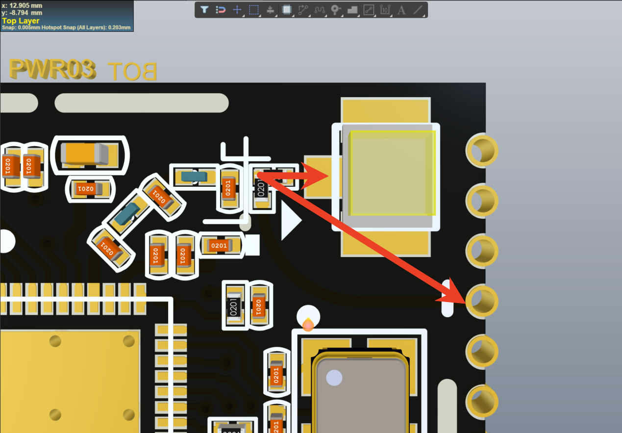
The first type features IPEX generation sockets on the module, which can be snapped together.
The second method involves using the top pins of the module to transmit the antenna signal to the bottom plate, and then designing the antenna form on the bottom plate.
By adjusting the welding states of resistors R3 and R4, the antenna connection mode of the MG24 module can be selected: IPX antenna or external PCB antenna.
| Antenna Solution | R3 | R4 |
|---|---|---|
| IPX ANT | × | √ |
| PCB ANT | √ | × |
×: No wielding.
√: Wielding.
Schematic Diagram:
Configuration Options
To better meet the requirements of different projects, this module offers the following hardware configurations for selection.
| Configuration Options | Applicable For | |
|---|---|---|
| Antenna method |
|
|
| radio-frequency power |
|
|
| Power consumption configuration |
| Low-power inductors are used in DC-DC power circuits, which can effectively reduce the static current of the module during deep sleep and receiving states, significantly enhancing the battery-powered device's endurance. |
| Crystal oscillator configuration1 |
|
|
| Crystal oscillator configuration2 |
|
|